| |
|

|
|
|
|
| |
|
|
|
|
Sample Digital Questions Asked in Interviews. Please contribute your questions. If you are looking for answers please refer to website FAQ |
| |
|
|
| |
 |
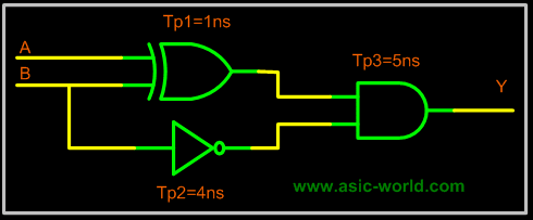
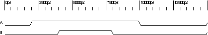
What is the output of AND gate in the circuit below, when A and B are as in waveform? Tp is the gate delay of respective gate.
|
| |
|
|
|
|
 |
| |
|
|
|
|
 |
| |
|
|
| |
|
Identify the circuit below, and its limitation.
|
| |
|
|
|
|
 |
| |
|
|
| |
|
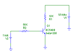
What is the current through the resistor R1 (Ic) ?
|
| |
|
|
|
|
 |
| |
|
|
| |
|
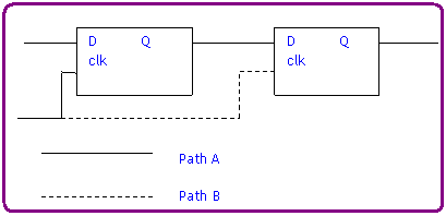
Referring to the diagram below, briefly explain what will happen if the propagation delay of the clock signal in path B is much too high compared to path A. How do we solve this problem if the propagation delay in path B can not be reduced ?
|
| |
|
|
|
|
 |
| |
|
|
| |
|
What is the function of a D flip-flop, whose inverted output is connected to its input ?
|
| |
|
|
| |
|
Design a circuit to divide input frequency by 2.
|
| |
|
|
| |
|
Design a divide-by-3 sequential circuit with 50% duty cycle.
|
| |
|
|
| |
|
Design a divide-by-5 sequential circuit with 50% duty cycle.
|
| |
|
|
| |
|
What are the different types of adder implementations ?
|
| |
|
|
| |
|
Draw a Transmission Gate-based D-Latch.
|
| |
|
|
| |
|
Give the truth table for a Half Adder. Give a gate level implementation of it.
|
| |
|
|
| |
|
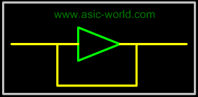
What is the purpose of the buffer in the circuit below, is it necessary/redundant to have a buffer ?
|
| |
|
|
|
|
 |
| |
|
|
| |
|
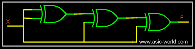
What is the output of the circuit below, assuming that value of 'X' is not known ?
|
| |
|
|
|
|
 |
| |
|
|
| |
|
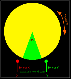
Consider a circular disk as shown in the figure below with two sensors mounted X, Y and a blue shade painted on the disk for an angle of 45 degree. Design a circuit with minimum number of gates to detect the direction of rotation.
|
| |
|
|
|
|
 |
| |
|
|
| |
|
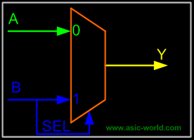
Design an OR gate from 2:1 MUX.
|
| |
|
|
|
|
 |
| |
|
|
| |
|
Design an XOR gate from 2:1 MUX and a NOT gate
|
| |
|
|
| |
|
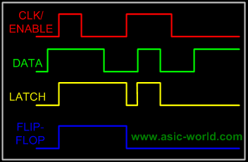
What is the difference between a LATCH and a FLIP-FLOP ?
|
| |
|
|
|
|
- Latch is a level sensitive device while flip-flop is an edge sensitive device.
- Latch is sensitive to glitches on enable pin, whereas flip-flop is immune to glitches.
- Latches take less gates (also less power) to implement than flip-flops.
- Latches are faster than flip-flops.
|
| |
|
|
|
|
 |
| |
|
|
| |
|
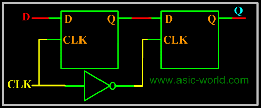
Design a D Flip-Flop from two latches.
|
| |
|
|
|
|
 |
| |
|
|
| |
|
Design a 2 bit counter using D Flip-Flop.
|
| |
|
|
| |
|
What are the two types of delays in any digital system ?
|
| |
|
|
| |
|
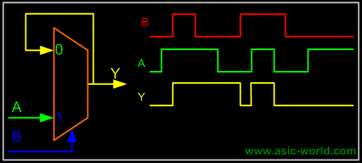
Design a Transparent Latch using a 2:1 Mux.
|
| |
|
|
|
|
 |
| |
|
|
| |
|
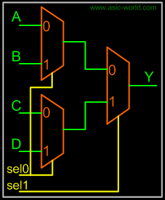
Design a 4:1 Mux using 2:1 Muxes and some combo logic.
|
| |
|
|
|
|
 |
| |
|
|
| |
|
What is metastable state ? How does it occur ?
|
| |
|
|
| |
|
What is metastability ?
|
| |
|
|
| |
|
Design a 3:8 decoder
|
| |
|
|
| |
|
Design a FSM to detect sequence "101" in input sequence.
|
| |
|
|
| |
|
Convert NAND gate into Inverter, in two different ways.
|
| |
|
|
| |
|
Design a D and T flip flop using 2:1 mux; use of other components not allowed, just the mux.
|
| |
|
|
| |
|
Design a divide by two counter using D-Latch.
|
| |
|
|
| |
|
Design D Latch from SR flip-flop.
|
| |
|
|
| |
|
Define Clock Skew , Negative Clock Skew, Positive Clock Skew.
|
| |
|
|
| |
|
What is Race Condition ?
|
| |
|
|
| |
|
Design a 4 bit Gray Counter.
|
| |
|
|
| |
|
Design 4-bit Synchronous counter, Asynchronous counter.
|
| |
|
|
| |
|
Design a 16 byte Asynchronous FIFO.
|
| |
|
|
| |
|
What is the difference between an EEPROM and a FLASH ?
|
| |
|
|
| |
|
What is the difference between a NAND-based Flash and a NOR-based Flash ?
|
| |
|
|
| |
|
You are given a 100 MHz clock. Design a 33.3 MHz clock with and without 50% duty cycle.
|
| |
|
|
| |
|
Design a Read on Reset System ?
|
| |
|
|
| |
|
Which one is superior: Asynchronous Reset or Synchronous Reset ? Explain.
|
| |
|
|
| |
|
Design a State machine for Traffic Control at a Four point Junction.
|
| |
|
|
| |
|
What are FIFO's? Can you draw the block diagram of FIFO? Could you modify it to make it asynchronous FIFO ?
|
| |
|
|
| |
|
How can you generate random sequences in digital circuits?
|
| |
|
|
| |
|
|
| |
|
|
|
|
|
| |
|
|